Introduction
I’ve had a Saturn board lying around for a long time. It’s a nice board with Spartan 6 series LX9 FPGA in CSG324 package, 512Mbits LPDDR memory which can run at upto 166MHz and lots of IOs. And it also has an FT2232H IC on it.
FT2232H is an interesting chip from FTDI, the manufacturer of well known USB-Serial ICs. It has 2 independent serial/FIFO channels, Channel A and Channel B. Each of these channels can be configured into various modes like UART, FIFO, JTAG, SPI, I2C etc. For Saturn, Channel A of FT2232H is reserved for FPGA configuration and flash programming. Channel B is generally used by user for UART communication. One thing to point out is that in Saturn, the control bus of Channel A is brought out to header, so we can use it for whatever purpose we desire.
In this article, we walk through technical details of FTDI’s Asynchronous FIFO interface which is necessary for this project, then we will proceed to the designing part where we design the FSM (or, algorithm in software parlance), and after that we simply implement our designed FSM in VHDL. Once VHDL coding is done, we verify our design through simulation. Finally, we test our design on hardware and benchmark the performace i.e, the transfer rate achieved.
FIFO Communication
FIFO is a common way of communication between two devices, specially if they are running at different speeds.
FT2232H FIFO Modes
FT2232H has two FIFO modes that a user can use for his/her purpose:
- Synchronous FIFO mode
- Asynchronous FIFO mode
Synchronous FIFO mode can push data at much faster rate. All signals in this mode are driven synchronous with the 60MHz clock sourced from FTDI itself. [marcan] reports having achieved 42MB/s of transfer rates with synchronous FIFO Mode [1]. Whereas, asynchronous FIFO mode can only transfer data at quite lower rate, because, well its asynchronous!
All points go in favour of synchronous FIFO mode, only except the fact that synchronous mode can only be used with Channel A of FT2232 and that in my Saturn board, Channel A is unfortunately unavailable to user because it is dedicated for FPGA configuration and flash programming. That leaves us Channel B of FT2232H available for use. But it only supports asynchronous FIFO mode. Bummer!
So what if we only have the choice of asynchronous mode with us! We can still transfer data from PC to FPGA over USB at reasonably good speed. People have achieved over 14MB/s transfer rate using this mode. So lets take a detailed look at it before we try writing VHDL code for it.
Asynchronous FIFO Mode
FT2232H datasheet[2] has a some details on asynchronous mode. Let’s first check out the pins/signals used for interfacing using this mode.
Pins:
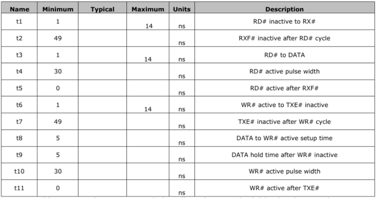
| Name | Type | Description |
|---|---|---|
BDBUS[7:0] |
I/O | D7 to D0 directional FIFO data. This bus is normally input unless RD# is low |
RXF# |
OUTPUT | When high, do not read data from the FIFO. When low, there is data available in the FIFO which can be read by driving RD# low. When RD# goes high again RXF# will always go high and only become low again if there is another byte to read. During reset, this signal is tri-state, but pulled up to VCCIO via an internal 200k ohms resistor. |
TXE# |
OUTPUT | When high, do not write data into the FIFO. When low, data can be written into the FIFO by strobing WR# high, then low. During reset this signal is tri-state, but pulled up to VCCIO via an internal 200k ohms resistor. |
RD# |
INPUT | Enables the current FIFO data byte to be driven onto D0…D7 when RD# goes low. Fetches the next FIFO data byte (if available) from the receive FIFO buffer when RD# goes high. |
WR# |
INPUT | Writes the data byte on the D0…D7 pins into the transmit buffer when WR# goes from high to low. |
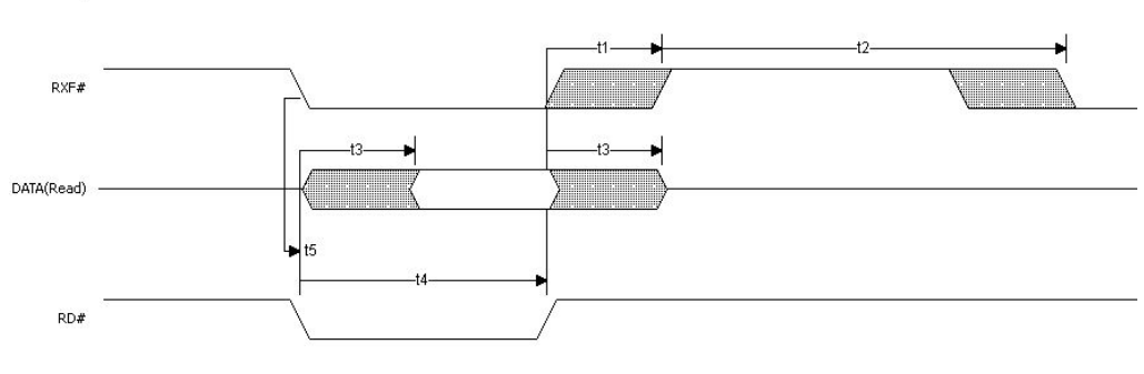
Read Timing Diagram:
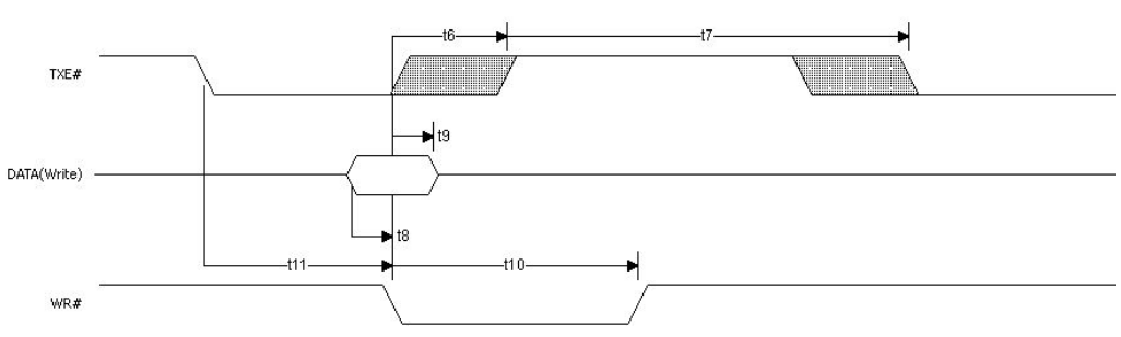
Write Timing Diagram:
Timing Parameters:
(All images above are from FT2232H Datasheet)
Design
Before doing anything, first we need to understand the timing diagrams shown above. Then we need to design our FSM as per our requirements. And finally, simply implement our FSM using either VHDL or Verilog or Migen. We’ll be using VHDL for this article.
Demostration Goal
The high-level goal of this article is to implement Asynchronous FIFO based communication between FPGA and FTDI FT2232H over USB. And how exactly will we be demonstrating this? For that, we need a low-level goal defined. Let’s just decide for this article, that we will be sending stream of data to the FTDI FT2232H over USB, and our FPGA board needs to read every byte of data from the stream, then increment the byte it just read, and finally send it back to our host PC via the same FT2232 chip using Asynchronous FIFO interface.
Understanding Timing Diagrams
Note: Signals with # in their name are active-low signals. That means, they are active when low, and inactive when high. Asserting an active-low signal means driving them low. Deasserting an active-low signal means driving them back to high, their inactive state.
When we send a byte of data from host PC over USB, to FTDI FT2232H IC, it gets stored in its internal receiver FIFO. We give commands through control sigals to read that data. Similarly, for sending something to host PC, we first write that data into FT2232H’s transmitter FIFO, after which FT2232H automatically handles sending it to host PC over USB channel.
Read Timings:
Whenever FT2232H has data available for reading in its FIFO, it asserts the RXF signal (drives it low since it is an active-low signal). This indicates to the user that FT2232H has some data available from host PC in its receiver FIFO, and that user is now free to read it whenever he/she wants to.
Now, for actually reading the data from FT2232H’s FIFO, user has to assert the RD signal (drive it low). From the timing diagram and the timing parameters table, we find that user is free to assert RD signal as soon as RXF is active (parameterized by t5 parameter in the table).
After the user has driven RD signal low, he/she isn’t supposed to read the data on DATA[7:0] lines instantly because there is no valid data on those lines! This is because FT2232H takes some time to fetch data from its receiver FIFO and put it on DATA[7:0] lines after RD is asserted. This time is parameterized by t3 parameter. The table says, t3 can be minimum 1ns to maximum 14ns. In digital designs, we design our systems according to worst-case situations. And here, the table says that in worst case, it may take for FT2232H almost 14ns to put data onto DATA[7:0] lines after we assert RD signal. So, to be always on safe side, we should read DATA[7:0] atleast 14ns after we have asserted RD signal.
Now, 14ns is some uncomfortable time duration for us, because Saturn has 100MHz clock oscillator. Which means we have resolution of only 10ns. [Note: Its not that simple though, there are many ways to improve this resolution. But for this article, let’s just go simple way] This means we can count in multiples of 10ns. So we have to wait for minimum 2 clock cycles (20ns) before reading DATA[7:0] lines. Please note that there is no maximum time limit for us to read the data. We are free to read it after 20ns, 30ns, 40ns etc. Any duration after 14ns is perfectly okay.
After reading data from DATA[7:0] lines, we have to deassert the RD signal so FT2232H can know that we have successfully read that data which it had put on DATA[7:0] lines and now it can remove that data from its FIFO. But, there is one more catch! We can’t deassert RD signal anytime. The timing parameter table says that active width of RD should be atleast 30ns. So if for example we were to read DATA[7:0] after 20ns of asserting RD, which is allowed, and if we then immediately deassert RD, it will result in violation of timings specifications, since RD has been active only for 20ns! So in this case, we should wait atleast 10ns more after reading data from DATA[7:0] lines before deasserting RD.
After deasserting RD properly, we are done for the reading part! We don’t need to care about anything else. FT2232H will handle rest for read part.
This whole process needs to be repeated to every byte that we want to read. For every byte, it starts with RXF being asserted by FTDI and ends with RD being deassserted by the user after which FT2232H automatically deasserts RXF also after some time (check timing diagram).
Write Timings:
Write process starts with FT2232H asserting TXE signal indicating that it is now ready to accept data from the user which needs to be transmitted to host PC over USB.
Although timing parameters table says that user can assert WR signal as soon as TXE is asserted by FT2232H, but in fact this is not allowed. There is one more catch!
For valid trasmission, user needs to put the data which is to be transmitted onto DATA[7:0] lines for t8 duration which is 5ns (also called setup time) before asserting WR and user also needs to keep/hold the data there for t9 duration which is again 5ns (also called hold time).
FT2232H will deassert TXE signal at maximum 14ns after WR is asserted by user. He/she needs to make sure that FT2232 has captured proper data by keeping the t8 and t9 timings mentioned in previous paragraph.
Same as for RD signal, WR also needs to be asserted for atleast 30ns before it can be deasserted by user. In our case, that means 3 clock cycles (100MHz clock, remember?).
As in case for read process, this process also needs to be repeated for every byte that we transmit.
TL;DR: Timings & Interfacing
Read process:
- Wait till
RXFis asserted (i.e, is driven low by FT2232) - Assert
RD - Read data from
DATA[7:0]lines after atleast 14ns - Deassert
RDafter atleast 30ns of its assertion
Write process:
- Wait till
TXEis asserted - Put data to transmit onto
DATA[7:0]bus - Wait for atleast 5ns
- Assert
WR - Hold the same data onto
DATA[7:0]bus for atleast another 5ns - Deassert
WRafter atleast 30ns of its assertion
FSM Design
| State | Description |
|---|---|
READ_IDLE |
Wait for RXF assertion. If RXF is asserted, assert RD and go to READ_PREWAIT state. |
READ_PREWAIT |
Wait for 2 clock cycles (20ns) then read data and go to READ_POSTWAIT |
READ_POSTWAIT |
Wait for 2 clock cycles (20ns), deassert RD and the go to WRITE_IDLE |
WRITE_IDLE |
Wait for TXE assertion. If TXE is asserted, put data onto DATA[7:0] bus and go to WRITE_PREWAIT |
WRITE_WAIT |
By the time we check that we are into WRITE_WAIT state, 1 clock cycle (10ns) has already elasped. So there is no particular requirement to wait for 5ns. So, just assert WR now and and wait for 3 clock cycles and move to WRITE_DONE |
WRITE_DONE |
Deassert WR and go to READ_IDLE |
IMPORTANT: Do not check for falling edge in above FSM! Instead, check for level. RXF and TXE might have already had their falling edge before you check for them, so your FSM gets stuck in IDLE state forever, because those RXF and TXE will never go high until you read/write but your code won’t read/write since it is still in IDLE state waiting for falling edge which has already occurred and which won’t occur again unless a read/write transaction is made! I initially made this same mistake, and most of the times my design would work but randomly fail after I would have transferred some number of bytes. It took sometime to figure out this bug!
Code
Note: All files related to this project are available in my github repository: https://github.com/rohitk-singh/ftdi-async-fifo
VHDL
--------------------------------------------------------------------------------
-- Author  : Rohit Singh
-- Module  : ft2232h - rtl
-- Project : FT2232H Async FIFO

-- License : The MIT License
-- Copyright © 2015, 2016, 2017, 2018 Rohit K. Singh (contact [AT] rohitksingh.in)
--------------------------------------------------------------------------------

library IEEE;

use IEEE.STD_LOGIC_1164.all;
use IEEE.NUMERIC_STD.all;

entity ft2232h is
	port(
		clk   : in    std_logic;
		rst   : in std_logic;

		-- FTDI FT2232H FIFO signals
		data  : inout std_logic_vector(7 downto 0);
		rxf_n : in    std_logic;
		txe_n : in    std_logic;
		rd_n  : out   std_logic;
		wr_n  : out   std_logic
	);
end ft2232h;

architecture rtl of ft2232h is
	signal data_o             : unsigned(7 downto 0) := (others => '0');
	signal data_i             : unsigned(7 downto 0) := (others => '0');
	signal data_en            : std_logic            := '0';

	signal rxf_n_meta            : std_logic            := '1';
	signal txe_n_meta            : std_logic            := '1';
	signal rxf_n_sync            : std_logic            := '1';
	signal txe_n_sync            : std_logic            := '1';

	signal rd_n_q                : std_logic            := '1';
	signal wr_n_q                : std_logic            := '1';

	signal reg      : unsigned(7 downto 0) := (others => '0');

	type states is (RD_IDLE, RD_PRE_WAIT, RD_POST_WAIT, WR_IDLE, WR_WAIT, WR_DONE);
	signal state : states := RD_IDLE;

	signal counter  : unsigned(1 downto 0) := "00";

begin

	-- Bi-directional logic
	data     <= std_logic_vector(data_o) when data_en = '1' else (others => 'Z');
	data_i   <= unsigned(data);

	rd_n <= rd_n_q;
	wr_n <= wr_n_q;

	-- Avoid metastability. Synchronize async signals  RXF and TXE
	synchronizer: process(clk)
	begin
		if rising_edge(clk) then
			rxf_n_meta            <= rxf_n;
			txe_n_meta            <= txe_n;
			rxf_n_sync            <= rxf_n_meta;
			txe_n_sync            <= txe_n_meta;
		end if;
	end process;

	main: process(clk, rst)
	begin
		if rst = '1' then
			state   <= RD_IDLE;
			rd_n_q  <= '1';
			wr_n_q  <= '1';
			counter <= (others => '0');

		elsif rising_edge(clk) then
			case state is
				when RD_IDLE =>
					if rxf_n_sync = '0' then
						rd_n_q <= '0';
						state  <= RD_PRE_WAIT;
					end if;
				when RD_PRE_WAIT =>
					counter <= counter + 1;
					if counter = "01" then
						state   <= RD_POST_WAIT;
						reg     <= data_i;
						counter <= "00";
					end if;

				when RD_POST_WAIT =>
				    counter <= counter + 1;
					if counter = "01" then
						rd_n_q  <= '1';
						state   <= WR_IDLE;
						counter <= "00";
					end if;

				when WR_IDLE =>
					if txe_n_sync = '0' then
						state   <= WR_WAIT;
						data_o  <= reg + 1;
						data_en <= '1';
					end if;

				when WR_WAIT =>
					wr_n_q  <= '0';
					counter <= counter + 1;
					if counter = "11" then
						state   <= WR_DONE;
						counter <= "00";
					    data_en <= '0';
					end if;

				when WR_DONE =>
					wr_n_q  <= '1';
					state   <= RD_IDLE;

			end case;
		end if;
	end process;

end rtl;
Simulation
Let’s see how my above design responds to my rudimentary testbench (Yeah, I suck at writing good tests)
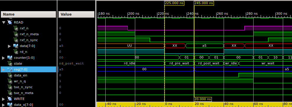
RD# active after RXF# assertion
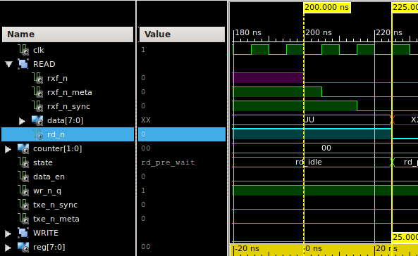
From the image above, we see that time delay between RXF# going low to RD# driven low by code is 25ns. Datasheet says it can be as low as 0ns. For fastest data transfer rate, it should ideally be 0ns. In real-world, this delay will vary from 20ns to 30ns, which comes from our current VHDL code.
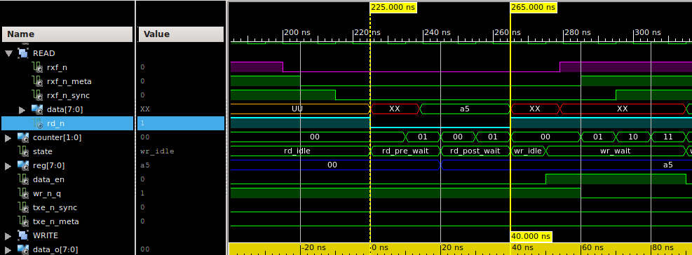
RD# asserted to reading data
From the above snip, we see that time delay from RD# driven low to actually reading data (check state and reg[7:0] signals) is 20ns. Datasheet specified atleast 14ns delay so we are good here also.
RD# pulse width
While datasheet says that minimum RD# pulse width should be 30ns, we are quite safe here with pulse width of 40ns.
Write data setup time
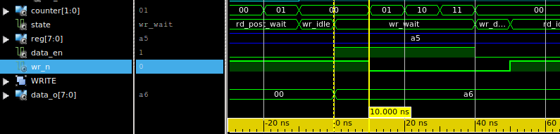
We put tx-data on DATA[7:0] lines 10ns before driving WR# low. So that satisfies datasheet’s minimum requirement of 5ns. We can notice here that a5 was read, and we are transmitting its incremented value i.e, a6.
WR# pulse width
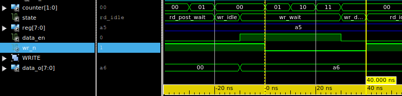
Same as in case of RD# signal, datasheet specifies minimum pulse width of 30ns and we are again on safe side with pulse width of 40ns.
So, our VHDL design seems to be working well in simulation. Its time to try it on actual hardware!
Running On Hardware
Note: All files related to this project are available in my github repository: https://github.com/rohitk-singh/ftdi-async-fifo
Clone/download my repository, then open the .xise project file in Xilinx ISE and build it. You might need to modify constraints in .ucf file if your board/schematic is different. Program the FPGA with generated bitstream and we are ready to test.
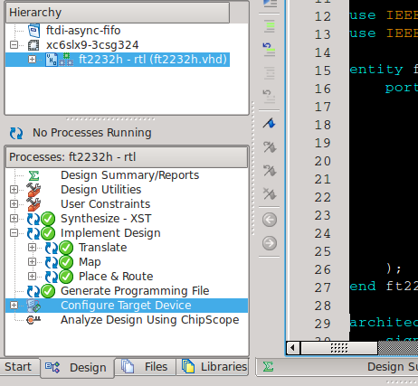
(No warnings, Yeah! That’s very rare in Xilinx ISE :p )
Test Setup
We need some way of sending data from host PC to FTDI, and reading data received from FTDI on host PC. The FTDI-FPGA part is handled by our design running on the FPGA.
There are many ways to do this on Linux and Windows. But, I’ll go with my own setup.
I’ll use Linux, Ubuntu 14.04 to be precise. I’ll use Python with pylibftdi library to send/receive data to/from FTDI.
So, for this test setup, you’ll need:
- Linux Host
- Python (already comes with most Linux distributions)
pylibftdilibrary properly set up and working
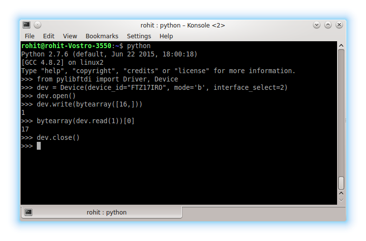
Using pylibftdi, it’s just a simple, few-lines-of-code job to test our project! So let’s fire up python!
from pylibftdi import Driver, Device

# Get list of all FTDI devices
dev_list  = Driver().list_devices()

# Print all devices
for device_ in dev_list:
    print device_
('FTDI', 'Saturn Spartan 6 FPGA Module', 'FTZ17IRO')
Above code lists out all FTDI ICs detected by the pylibftdi library. We can see my Saturn board has been detected by it.
Now let’s open this device, write something to it and read back same number of bytes to test if our VHDL design for FTDI Asynchronous FIFO communication is working fine or not.
# Create Device instance: Channel B in binary mode
dev = Device(device_id="FTZ17IRO", mode='b', interface_select=2)

# Open the instantiated device
dev.open()

# Write value 16 to FTDI over USB, returns number of bytes written
dev.write(bytearray([16,]))

# Read one byte
rx_data =  bytearray(dev.read(1))

# Print the byte received. Should be 16+1 i.e, 17
print rx_data[0]

# Close device after use
dev.close()
17
Yes! Our design is working! We sent 16 and received 17 as expected! Check the screenshot below for actual proof!
Performance & Benchmarking
In the last section, we just did a simple test. We sent one byte, received one byte and verified whether the received byte was indeed incremented by one or not. But, this is not sufficient to prove the reliability of our design.
We need to do more rigorous testing to prove that our design works reliably. In this section we will subject our design to much more data than just 1 byte! Let’s see my simple benchmarking code.
#! /usr/bin/python

import sys, os
import time
import random

from pylibftdi import Driver, Device

dev_list  = Driver().list_devices()
if len(dev_list) != 0:
    print "Following devices found:"
for device_ in dev_list:
    print device_

dev = Device(device_id="FTZ17IRO", mode='b', interface_select=2)
dev.open()


epochs = 1024*10
BLOCK_LEN = 2048
tx_data = bytearray([ random.randrange(0, 256) for i in range(BLOCK_LEN)])
ts = time.time()
while epochs:

    dev.write(tx_data)
    rx_data = bytearray(dev.read(BLOCK_LEN))

    #print "Epoch: {}".format(epochs)
    failed = False
    for i in range(BLOCK_LEN):
      if ((tx_data[i]+1)%256) != rx_data[i]:
        print "Epoch: {}".format(epochs)
        print "[Test]: Data verification failed! , tx_data : ", tx_data[i], " =/= rx_data : ", rx_data[i]
        failed = True
        print "Breaking..."
        break
    if failed:
        break

    epochs -= 1

dev.close()
te = time.time()
print "Time {}".format(str(te-ts))
This code will send a random generated block of data of length BLOCK_LEN total of 10240 times and verify whether we have received expected data or not. I’ve chosen BLOCK_LEN to be 2048, so in total we are sending 20MB (Mega Bytes) of data to the FPGA, which is quite a large amount! We are also receiving 20MB of data and verifying its correctness. We will also measure the time it takes to complete the whole operation.
Code runs successfully without any verification error! And we get the following output:
Following devices found:
('FTDI', 'Saturn Spartan 6 FPGA Module', 'FTZ17IRO')
Time 10.9798371792
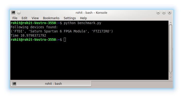
That’s around 1.8 MB/s transfer rate considering only transmitted data! If we take into account data in both directions, then transfer rate is actually twice of that, i.e, around 3.6 MB/s! That’s quite satisfactory performance for me. We can improve it further by using C/C++ interface and squeezing the VHDL code further!
Conclusion
This project was quite interesting to me, as I wanted to see for myself how can I use FTDI’s Asynchronous FIFO interface. In this article, we went into some basic theory, then designed our FSM/algorithm based on that theory, implemented it in VHDL, simulated it, and finally ran it on hardware. We did proof-of-concept tests and benchmarks on our design. And, yeah we achieved 1.8 MB/s transfer rate!
References
- http://www.eevblog.com/forum/microcontrollers/ftdi-ft232h-in-synchronous-fifo-questions/msg671602/#msg671602
- http://www.ftdichip.com/Support/Documents/DataSheets/ICs/DS_FT2232H.pdf